In the dynamic world of technology, LED (Light-Emitting Diode) displays have emerged as a remarkable innovation, redefining the way we perceive visual communication. Behind their stunning visuals lies a meticulous craftsmanship of encapsulation techniques, which not only enhances their performance but also ensures durability and longevity. This article delves into the intricate details of six commonly used LED display encapsulation methods, shedding light on their merits and limitations. Moreover, it envisions the future prospects of this rapidly evolving field.
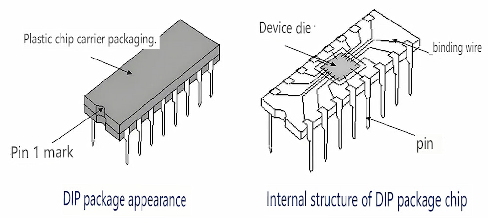
I. Dual In-line Package (DIP) Encapsulation:
1. Development Origin: DIP packaging technology originated in the late 1990s and was the primary packaging method for early LED displays.
2. Manufacturing Process: LED chips are directly inserted into the PCB board and fixed through soldering to form an LED display module.
3. Working Principle: Current passes through the circuit on the PCB board to drive the LED chips to emit light and form a display image.
4. Product Features: Simple process, low cost, but relatively lower luminous efficiency and heat dissipation.
5. Application Areas: Widely used in indoor displays, billboards, etc., in the early stages.

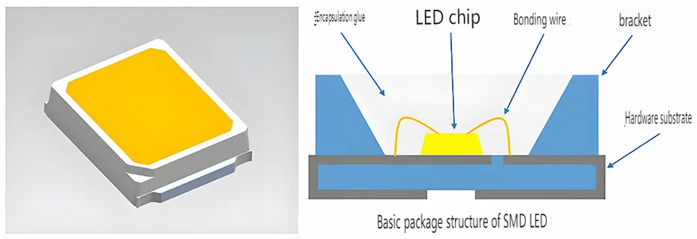
II. Surface-Mount Device (SMD) Encapsulation:
1. Development Origin: SMD packaging technology emerged with the reduction of LED display pixel pitch and has become one of the most common packaging methods in the market.
2. Manufacturing Process: LED chips are packaged into individual lamps and then mounted and soldered onto the PCB board.
3. Working Principle: Current passes through the circuit on the PCB board to drive the SMD chips to emit light, forming high-definition display images.
4. Product Features: Mature technology, good heat dissipation, relatively low production cost, suitable for displays with various pixel pitches.
5. Application Areas: Widely used in indoor and outdoor displays, billboards, stage backgrounds, etc.

III. Chip-on-Board (COB) Encapsulation:
1. Development Origin: COB packaging technology was developed to further reduce the pixel pitch of LED displays.
2. Manufacturing Process: Multiple LED bare chips are directly mounted on the PCB board and then encapsulated as a whole with resin.
3. Working Principle: Current passes through the circuit on the PCB board, directly driving the bare chips to emit light, forming high brightness and high-definition display images.
4. Product Features: No support structure, compact design, high luminous efficiency, good heat dissipation, suitable for high-definition displays.
5. Application Areas: Mainly used in high-definition indoor displays, commercial showcases, home theaters, etc.

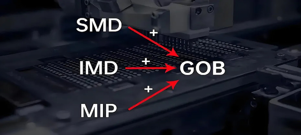
IV. Glue-on-Board (GOB) Encapsulation:
1. Development Origin: GOB technology is a new packaging technology introduced to address the protection of LED display chips.
2. Manufacturing Process: The PCB board and LED chips of conventional LED displays are treated with glue filling to form a protective layer.
3. Working Principle: Current passes through the circuit on the PCB board, driving the chips to emit light. The glue layer provides protection and enhances luminous efficiency.
4. Product Features: Excellent protection performance, high luminous efficiency, good heat dissipation, suitable for displays in harsh environments.
5. Application Areas: Mainly used in outdoor displays, billboards, stadiums, etc.

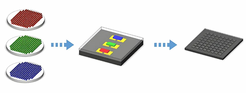
V. Micro/Mini LED Integrated Packaging (MIP) Technology:
1. Development Origin: MIP packaging technology is an innovative technology developed for Micro/Mini LED chips.
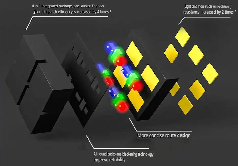
2. Manufacturing Process: Micro/Mini LED chips are cut into single or multiple chips, and the display assembly is completed through processes such as mass transfer, packaging, and cutting.
3. Working Principle: Current passes through the tiny LED chips, driving them to emit high-definition and high-brightness display images.
4. Product Features: Extremely small pixel pitch, capable of achieving ultra-high-definition displays, suitable for the high-end display market.
5. Application Areas: Mainly used in automotive displays, virtual cinematography, high-end commercial Led wall showcases, etc.

VI. Integrated Molded Device (IMD) Array Encapsulation:
1. Development Origin: IMD packaging technology can be seen as an intermediate step between SMD discrete devices and COB.
2. Manufacturing Process: Multiple LED chips are integrated into one package structure, forming an array arrangement.
3. Working Principle: Current passes through the circuit in the package structure, simultaneously driving multiple LED chips to emit light and form a display image.
4. Product Features: High pixel density, low cost, suitable for the mid-to-high-end display market.
5. Application Areas: Mainly used in indoor displays, billboards, and commercial showcases.

Future Outlook:
As LED display screen encapsulation techniques evolve, the future holds exciting possibilities. The convergence of new materials, advanced manufacturing processes, and emerging technologies such as quantum dots and organic LEDs will likely revolutionize display technology. We can anticipate displays that are not only visually stunning but also energy-efficient, flexible, and seamlessly integrated into our daily lives.
Conclusion:
Unveiling the artistry of LED display encapsulation reveals a world where technology meets creativity, precision, and imagination. The six examined techniques provide a glimpse into the versatility and potential that LED displays possess. With the rapid progress in this field, it is certain that LED display billboard will continue to captivate audiences and reshape the way we interact with visual information. So, brace yourself for a future filled with awe-inspiring displays that blur the line between reality and imagination.


 language :


